
Research on QSPF28 SR4 Encapsulation-COB Package 2022
The traditional single-channel 10 Gb/s or 25 Gb/s rate optical module adopts SFP (Small Form-factor Pluggable, small form factor pluggable) package shell, the size is 56.5 mm × 13.4 mm × 8.5 mm, the electronic chip and TO (Through-hole) packaged light emitting and receiving components are welded to the PCB board to form a photoelectric conversion module with transceiver function. The 100 Gb/s optical module mainly adopts the QSFP (Quad Small Form ⁃factor Pluggable) package, with a size of 76.4 mm × 18.35 mm × 8.5 mm, and has four 25 Gb/s signal transmission channels. If the traditional method of designing SFP is used to solder electronic chips and discrete optical components to the PCB board to design 100G SR4, 4 groups of electronic chips and optical components are soldered to the PCB board together, regardless of the increased space caused by the increase of single-channel rate. Influence, it needs about 4 times the space of SFP size. But QSFP is only slightly larger than SFP, so 100 Gb/s optical modules use traditional design.

The solution cannot achieve the QSFP miniaturized housing package.To solve the design of parallel optical modules, it is necessary to consider the method of optoelectronic integrated packaging. Optoelectronic integrated packaging is to integrate optical devices and electronic bare chips together in a small space. To achieve integrated packaging, it is necessary to consider the realizability of packaging to find a suitable method for optoelectronic hybrid packaging. For the integrated packaging of parallel optical modules, some manufacturers use the electrical bending method of placing the optoelectronic integrated device on the flexible board and connecting the flexible board to the PCB. This technology draws on the Flip Chip packaging technology. Flip Chip packaging technology places bare chips of various solder face down on corresponding PCB pads, usually using special equipment from the wafer. Remove the chip, turn it upside down and place in a small Waffle Pack. FlipChip packaging technology further improves the pin packaging density. It makes the connection between the pin and the pad shorter, which is beneficial to reduce the influence of signal integrity problems such as parasitic parameters caused by high-speed signal connections. However, the reliability inspection is more complicated, and can only be inspected with the help of X-ray or ultrasonic principles.
The complexity, difficulty and precision are very high, requiring a high accumulation of process technology. In addition, the manufacturing precision of the Flip Chip packaging fixture is relatively high. To realize the optoelectronic integrated packaging of parallel optical modules, the problem of high-precision fixtures and process equipment must be solved, and the dependence on automatic control and image recognition technology is also high.
The integrated packaging of parallel multi-channel optical devices and electrical chips determines the success or failure of the research and development of 100G SR4 parallel optical transceiver modules. In the design scheme of this paper, COB (Chip On Board) packaging technology is used, the chip is directly pasted to the PCB board through adhesive or solder, and the interconnection between the chip and the PCB board is realized by wire bonding to realize the device packaging. COB packaging can greatly increase the package pin density. At the same time, based on COB packaging technology, to improve the coupling efficiency, optical bending technology is used to realize fiber coupling; in the specific coupling process, the active coupling method is used to reduce the cost and improve the coupling accuracy; the process operation of the entire packaging technology is simple, There is no need to invest in other fixtures and process equipment for high-precision packaging. This packaging technology based on parallel optical modules is called COB optical bending active coupling packaging technology.
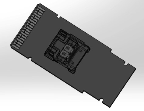
Figure 1: COB package diagram
SR4 parallel optical modules are mainly used for short-distance interconnection between switches and switches in data centers, and between switches and storage. IEEE Std802.3bmTM [7] defines the index requirements of Ethernet 100GBase-SR4 transmission. The 100G SR4 parallel optical module adopts 850 nm wavelength and a single channel transmission rate of 25 Gb/s. The transmitting end uses 4 channels of VCSEL (Vertical Cavity Surface Emitting Laser, vertical cavity surface emitting laser) to emit light, and the receiving end uses 4 channels of PD (Photo- Diode, photodiode) to receive light.
According to the requirements of SR4 parallel optical transmission, the photoelectric conversion of 4 channels of 25 Gb/s signals is realized in the optical module package such as QSFP, and then the parallel transmission of 4 channels of optical signals is realized. The optoelectronic devices in the parallel optical module include 4-channel VCSEL array, 4-channel PD array, transmitting VCSEL driver chip, and receiving TIA/LA (Trans ⁃ Impedance Limiting Amplifier) chip. For single-channel 25 Gb/s high-speed transmission, to improve signal quality, both the VCSEL driver and the TIA/LA chip need to integrate the CDR (Clock Data Recovery) function. The schematic diagram of a typical parallel optical module is shown in Figure 1. At the transmitting end, the transmitting driver chip drives the VCSEL array, modulates the electrical signal into the optical signal and couples it into the optical fiber for transmission to realize electrical-optical conversion. At the receiving end, the light transmitted by the optical fiber is coupled to the PD array and converted into a current signal. The current signal is amplified and processed by TIA/LA to demodulate a differential electrical signal carrying information to realize optical-to-electrical conversion. The MCU realizes the functions of control, data storage, protocol function and signal monitoring; at the same time, the MCU also forms a closed-loop active coupling control loop with the coupling control machine, providing the software and hardware technical support for active coupling for the COB package. The MCU communicated with the TIA/LA and VCSEL driver chips through I2C before, and the TIA/LA and VCSEL driver chips were used as slaves; the MCU, as the I2C master, was implemented by simulating I2C through the GPIO port of the MCU.

Figure 2: COB package structure
To realize the optoelectronic integrated package of 100G SR4 optical module, it is necessary to package the TIA/LA chip, VCSEL driver chip, VCSEL array and PD array as shown in Figure 2 in a small space and establish their electrical connection, and connect with the MCU through the reserved interface. Establish a physical connection to the PCB board. In the design scheme of the 100G SR4 optical module in this paper, the small space is directly placed on the PCB, that is, the TIA/LA chip, VCSEL driver chip, VCSEL array and PD array are directly pasted to the PCB of the optical module through solder. As the name implies, Chip on Board (chip on board or chip on board package). The VCSEL array and the optical fiber, the PD array and the optical fiber use the lens to realize the optical bending method, the light of the VCSEL array is coupled into the optical fiber, and the light transmitted by the optical fiber is coupled to the PD array; the coupling process technology adopts the method of active coupling. This process technology and packaging method form a complete set of optoelectronic integrated packaging technology, also called COB packaging technology.